(Click title above to download PDF)
Introduction
This Application Note is intended to highlight the workings of GigaIO’s FabreX™ networking technology so as to enable readers to conceive of the architecture towards designing their solutions.
In today’s world the general perception of people of ubiquitous connectivity as experienced in their daily lives suggests the presence of a networking infrastructure supporting this phenomenon. This elusive infrastructure is where FabreX fits in. The massive demands for compute and storage resources to address the burgeoning applications such as Big Data, AI, ML/DL, etc. is made possible only with networking technologies such as FabreX.
Evolution of FabreX
With the advent of the microprocessors came microcomputers and then PCs and now servers. Workloads that used to be performed by Mainframe Super Computers and Minicomputers evolved into being performed by Servers with the processing being distributed amongst a set of servers working in unison.
Server architecture evolved from PCs where a motherboard provided the processor ecosystem with its ability to connect to various I/O resources. This interconnect technology went through numerous rounds of technological evolution. The industry has now settled on a standard originating almost two decades ago on an interconnect technology called Peripheral Component Interconnect Express (PCIe). This interconnect constitutes a very robust communication protocol encompassing the best of many contemporary communication technologies when it was established. The industry also had the foresight to stipulate a migration path for this communication standard on adapting progressively newer and more powerful generation of the technology.
FabreX technology is built on the back of PCIe technology.
Insight into the Operation of PCI Express
Any processor within a Server primarily communicates with two hardware resources, namely I/O and Memory respectively. As a result, interconnects between the processor and the resources are required to support only two modes of operation. They are Memory and I/O transactions.
However, over time it was realized the fundamental read/write operations to I/O devices are no different than read/write operations to Memory. Consequently, the industry has terminated the support of I/O transactions for any new design. It was replaced by Memory operations to I/O devices and is appropriately termed as MMIO (Memory Mapped IO).
Another phenomenon which was extremely difficult during the early days of PCs was the process of integrating I/O device drivers with the OS. Every type of I/O device required its own I/O address space for mapping its registers for communicating with the processor; and furthermore, if the I/O device needed memory to be visible to the processor then it too had to be mapped into the processor’s address space. The real issue in these scenarios turned out to be the dire need to resolve all conflicts in resolving the requirements of the I/O devices and orchestrate an assignment of these resources in the processor’s address space in a seamless manner.
To address this precise situation the industry came up with Plug-n-Play feature that needed to be supported by all I/O devices. This works by letting the processor know upon its query of resources needed by all of the I/O devices under its domain. This way the processor could resolve the contention amongst all of the I/O devices and assign specific unique address spaces to the individual I/O devices thereby allowing it to communicate at will and unfettered with all of them.
In PCIe systems the technique to accomplishing this is called Enumeration. The software module dedicated to carry out this task is called BIOS.
The Net Result
In a PCIe system all transactions from the perspective of the processor are confined to memory transactions. This even includes Interrupt operations which are Memory Write operations to specific system memory locations.
After the enumeration process all I/O resources appear as memory to the processor. Consequently, all communications between the processor and these resources are purely memory transactions. Also, by extension, I/O resources that are capable of initiating memory transactions also have the ability to communicate with other I/O resources; a typical instance of this will be an integrated DMA controller engine on an I/O resource. Processors requiring communicating with other processors do not have the ability to directly communicate with each other. However, this is done indirectly with memory to memory transfers initiated by respective processors with their respective memory resources.
The FabreX Solution
FabreX, which is a network fabric, transforms all resources connected to the fabric as unique memory resources. The word ‘unique’ in this context implies unique memory address space and an aperture parameter stipulating a memory window size without of course allowing for any overlap of these spaces. This technique forms the genesis of FabreX technology.
FabreX virtualizes all devices attached to it by transforming them as unique memory resource windows in a 64-bit Global Virtual Address Space. Communication between these resources takes place with PCIe memory transactions operating at PCIe native speeds.
Application Example
All of FabreX applications without exception entails first transforming hardware resources to appear as memory resources, which implies assigning a memory address and an aperture defining the memory window size.
The implementation of this method involves the generation of a Virtual Address Map where each of these memory resources carve out a memory window for itself with absolutely no overlap. The Physical Address to Virtual Address transformation is done via Address Translation logic at every port.
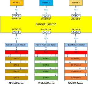
Figure 1 shows an example of GigaIO’s FabreX Switch providing the interconnect fabric between 3 Servers and 3 Resource server boxes, each of which in this example is of different type.
Every FabreX switch has a Control Plane and a Data Plane.
The Control Plane consists of x-86 processor ecosystem which controls the FabreX Data Plane and conducts various housekeeping and BMC (Board Management Control) services.

Figure 1 –GigaIO FabreX Switch
The Data Plane consists of ports, which are an integral part of the FabreX switch. Ports provide the attachment mechanism between Servers and I/O Resources with the switch. The Data Plane implements the Switching function of PCIe traffic between the ports. The communication between ports happen totally unblocked at PCIe native speeds with byte latency of 11nsec when configured for 128 Gigabits/sec.
The ports can be configured from any of the three following data rates:
- 32 Gigabits/sec (x4 PCIe Lanes)
- 64 Gigabits/sec (x8 PCIe Lanes)
- 128 Gigabits/sec (x16 PCIe Lanes)
The Resource servers shown attach to the FabreX Switch via a FabreX Network Adaptor that is of the form factor of half-high and half-length PCIe card. Also, the Servers have similar FabreX Network Adapter resident in them, which is not shown in the figure. These Adapters provide the attachment via PCIe signaling between the FabreX Switch and the Server and/or I/O Resource server backplanes.
Theory of Operation
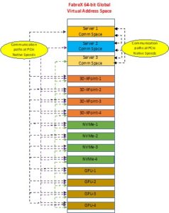
Figure 2 shows how all of the resources involved in this configuration are assigned unique Virtual Memory Windows within the 64-bit Global Virtual Address space. This is performed by Address Translation logic residing on every port of the FabreX Switch. The Switch Controller is responsible for assigning these unique addresses.
Figure 2 – Virtual Memory Windows

The communication between the Servers’ system memory windows can only take place by each Server Reading/Writing to the system memory of the others. The I/O resources of the I/O Resource Servers may also initiate similar memory transactions.
The Root Complex Processor (RCP) of the individual Resource servers perform the enumeration of their respective I/O devices and then gracefully gets out of the way after establishing a memory path conduit to the FabreX Switch via the FabreX Network Adapter. It also passes some parameters specific to the I/O devices to the Control Plane of the Switch. All of this happens at Boot time.
The assignment of unique Virtual Memory Windows corresponding to the Physical memory of Server system memory and/or Resource server is performed by the Control Plane in coordination with the Server and/or Resource server.
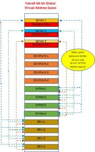
Figure 3 – FabreX DMA Paths

Figure 3 shows the various DMA paths of I/O devices via the FabreX Switch that are capable of initiating memory transactions. These DMA paths are in addition to the peer to peer DMA paths between I/O devices via the backplane of a Server where these devices reside if they are able to initiate memory transactions.
The I/O devices capable of initiating Memory transactions in this example are the NVMe drives and the GPU cards. NVMe drives cannot communicate amongst themselves and consequently the paths shown are directly to the Server system memory
The GPU cards on the other hand have the ability to transfer data in DMA fashion to other GPUs. The DMA paths shown in this figure are via FabreX between GPU cards in the I/O Resource server and GPU cards resident on the Server and/or to Server system memory.
The DMA paths between GPU cards within the Resource server are not shown in this diagram.
Conclusion
FabreX is the only technology currently available that allows for communication between all resources attached to the fabric to take place at PCIe native speeds
The latency incurred in these communication paths are the lowest and unmatched in the industry since there are no communication protocol transformation involved with the I/O signaling emanating from the RCP and the communication path to I/O resources including memory.
FabreX is the only communication technology in the industry today that allows for true memory centric operations of Load and Store between Servers and I/O devices across the fabric.
Since data transfers happen at PCIe native speeds, the bandwidth of the communication path of FabreX is identical to the bandwidth of the I/O signaling path emanating out of the processor.
In order to accommodate legacy application software, the Middleware sits between the Application and the data transport mechanism to make customer applications appear as Plug-n-Play. However, the data transport primitive uses the technology in the manner described in this Application Note.
About GigaIO
GigaIO has invented the first truly composable cloud-class software-defined infrastructure network, empowering users to accelerate workloads on-demand, using industry-standard PCI Express technology. The company’s patented network technology optimizes cluster and rack system performance, and greatly reduces total cost of ownership. With the innovative GigaIO FabreX™ open architecture, data centers can scale up or scale out the performance of their systems, enabling their existing investment to flex as workloads and business change over time. For more information, contact the GigaIO team at info@gigaio.com or Schedule a demo.